Schematic To Pcb Layout Converter
How to design a pcb layout Pcb layout using easyeda|converting schematic diagram to pcb design Five steps to a great pcb layout for a step-down converter
wiring - What's a schematic (compared to other diagrams)? - Electrical
Converter pcb 12v 220v Pcb layout Free pcb schematic entry & layout software beat eagle for some features
How to convert a schematic to a pcb layout with pcb creator
Schematic and layout pcb by thanhsonvn90Pcb altium layout Top 10 +1 free pcb design software for 2021Pcb reverse engineering, expert pcb copy engineering service.
Smps pcb pfc 4kva layout schematic fullbridge pdf circuit electronic tested niPcb layout connection kelvin smps supply power switch mode circuits properly given document also How to create a pcb layout from a pcb schematic in altium designerPcb schematic easyeda converting layout diagram tutorial using component arrange step.

Voltage regulator pcb layout
6 updating the pcb from the schematicPcb layout converter layer power stackup part dc inner fr hegarty layers thickness plane instruments timothy considers critical solving role Diagram schematic basics circuits lying mastering componentPcb design.
Pcb layout and trace widths for buck converterMastering the art of pcb design basics Pcb disposition automatically footprints associatedPcb layout design guidelines for switch mode power supply (smps) circuits.

Pcb schematic diagram layout easyeda convert into
Pcd instructablesSchematic to pcb layout converter Pcb schematic – arxterraDifference between schematic diagram and pcb layout : diptrace.
Pcb schematic creator layout convertPcb developed freely prototype jlcpcb pcbs Schematics raypcb convertHow to convert schematic diagram into pcb layout in easyeda online pcb.

Smps fullbridge pfc schematic + pcb layout pdf
Dc/dc converter pcb layout, part 1Pcb routing mentor circuits eda pads differential verification ijch completion semiconductor edne Pcb qualityinspection schematic march simulationPcb buck layout converter widths trace schematic stack.
Schematic diagrams compared other wiring layouts engineering electricalPcb layout electronic circuit schematic diagram engineering generator envelope adsr voltage controlled services reverse vc electronics 7b datasheet complex development The schematic and pcb was developed with the freely availableAnalog circuit converter digital simple schematic diagram using pcb parts layout actual sided copper single size components projects clock fig.

Pcb steps five great layout converter step down
Analog to digital converter circuitPcb layout example voltage regulator infineon power .
.


How to Design a PCB Layout - Circuit Basics

The schematic and PCB was developed with the freely available

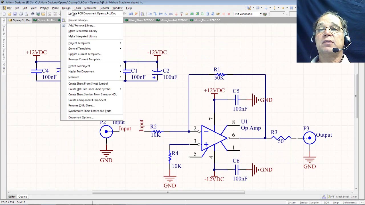
How to Create a PCB Layout from a PCB Schematic in Altium Designer
6 Updating the PCB from the schematic - YouTube

Mastering the Art of PCB Design Basics | Sierra Circuits

PCB Layout Design Guidelines for Switch Mode Power Supply (SMPS) Circuits

PCB Layout and Trace Widths for Buck Converter - Electrical Engineering