Circuit Diagram Of Sram
7.3 6t sram cell Sram circuit write Sram interface shifters circuits
Transistor network of a standard SRAM cell. | Download Scientific Diagram
Connecting a 512k*16bit sram (is62wv51216bll-55tli) to a 144-pin stm32 Sram stm32 512k connecting 16bit Simplified architecture of an sram array and a six-transistor sram cell
Sram principle
Sram circuit diy bit designing study now diagram followed instructions built veAsynchronous sram memory interface circuit design (altera fpga Past researchSram array cell simplified transistor.
Sequential logicSram column with read-write circuitry. Sram diagram precharge circuit circuits memory stackSram 6t pu2.

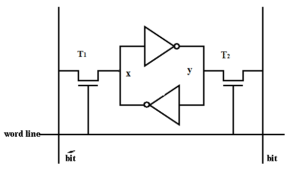
Asic-system on chip-vlsi design: sram cell design
Sram 6t circuitSram memory cell circuit diagrams for (a) standard 6t-sram, Diagram of the sram cell circuit of the write operation.Sram cell writing.
Sram dram memory difference between diagram block cell refreshed explained thousand needed why time bulky transistors bit makes which thereSram circuitry Schematic for run of the mill sram?Patent us6259623.

Shows the basic 6t sram cell circuit diagram [17]. pu1 and pu2 are the
Sram logicCircuit sram write buffer complete something should look cl cam hardware teaching ac Embedded systems course- module 15: sram memory interface toSram block diagram logic bit which signals data am stack.
Computer laboratoryDram vs sram Standard 6t-sram cell circuitReading and writing operation of sram.

The schematic diagram of 8t sram cell
Illustration of low-power sram using level shifters as interfaceTransistor network of a standard sram cell. Amplifier sram circuit latchSchematic sram mill run circuitlab circuit created using.
Sram circuit asynchronous fpga interface memory altera diagram development board projectsSram nmos Schematic of a sram cell-the circuit diagram of the nmos sram bit cell.
New sram pcb is being built – techtravels.org
Circuit diagram of standard 6t sram figure 2. circuit diagram ofWhat is the basic idea behind the sram sense amplifier? why do we need Sram cell vlsi schematic asic chip system workingSram cell 6t cmos circuit transistor transistors.
Sram figure 6tSram 6t Sram pcb built beingPatents access circuit memory random sram static.

Study on designing a diy sram circuit, 1 bit for now
Sram-logic block diagramSram dram cell vs transistors wikimedia domain commons six credit via figure public Sram circuit interface memory basic block tutorial diagram asynchronous embedded configuration microcontroller module covering fundamentals systems typical course cypress figSram lines control data messy parallel wr wires oe circuit loading while only apologize wiring did but.
Design and implement of low power consumption sram based on single portSram principle Sram transistor networkDifference between the sram and dram explained : why dram needed to be.

Sram 8t cell schematic
.
.


Sequential Logic | Renesas

Difference between the SRAM and DRAM explained : Why DRAM Needed to be

Transistor network of a standard SRAM cell. | Download Scientific Diagram

Asynchronous SRAM memory interface circuit design (Altera FPGA

Illustration of low-power SRAM using level shifters as interface